Lattice Merges Fixed Hardware Security with FPGA Flexibility
Lattice MachXO5D-NX: Secure and Powerful FPGAs for the Evolving Edge
Lattice Semiconductor, a leading name in low-power, low-cost Field Programmable Gate Arrays (FPGAs), introduces the MachXO5D-NX family. This mid-range offering combines cost-efficiency and low-power consumption with a comprehensive set of peripherals and robust security features, making it ideal for secure edge devices.

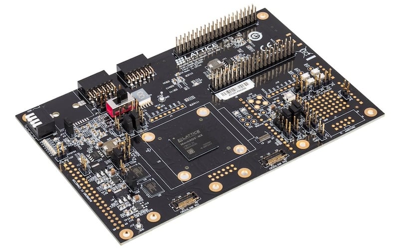
MachXO5 development board.
Security by Design: Balancing Flexibility and Protection
FPGAs present inherent security challenges due to their programmability. However, this very characteristic also allows for post-deployment security updates. Lattice addresses this by equipping the MachXO5D-NX family with built-in hardware encryption and security features. This design philosophy grants the flexibility of an FPGA with the security of fixed-function hardware. On-chip flash memory and hardware encryption capabilities streamline device design by reducing the number of required chips, mitigating code capture risks during loading.
The MachXO5D-NX Family: A Trio of Secure Powerhouses
The MachXO5D-NX family consists of three members, each offering a range of logic cells:
- FMXO5-25: Equipped with 27,000 logic cells.
- LFMXO5-55T: Provides 53,000 logic cells.
- LFMXO5-100T: Offers a maximum of 96,000 logic cells.
Beyond logic cells, the family boasts additional features:
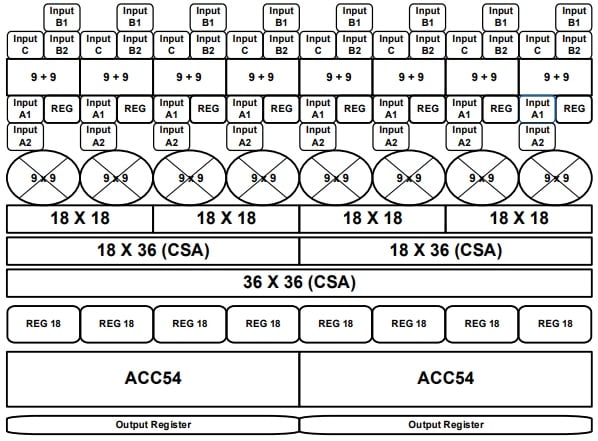
- 20 to 156 sysDSP 18x18 Multipliers: Enables efficient edge AI and other math-intensive applications.
- 1.9 Mb to 7.3 Mb Embedded RAM: Provides a range of options for on-chip memory needs.
- 200 to 300 High-Performance I/O: Supports various interface requirements.

MachXO5-NX DSP block and register layout.
Unveiling the Connectivity Powerhouse Within
The MachXO5D-NX family integrates a comprehensive set of built-in peripherals, including:
- MIPI D-PHY (CSI-2, DSI): Facilitates high-speed data transfer for camera and display applications.
- LVDS, SLVS, subLVDS: Supports various low-voltage differential signaling standards.
- Gigabit Ethernet, PCIe (Gen1 and Gen2): Enables high-bandwidth network connectivity.
Flexible Memory Options and Development Tools
The chips come equipped with embedded flash memory for on-chip multi-boot capabilities, along with dedicated user flash memory (UFM) for custom data storage. In addition to onboard distributed RAM (EBR and LRAM) blocks, the series boasts built-in interfaces supporting DDR3, DDR3L, and LPDDR4 memory standards at speeds up to 1066 Mbps.
Development is streamlined with the Lattice Radiant design suite and synthesis libraries from popular design tools. Furthermore, Lattice offers a comprehensive library of pre-engineered soft IP cores and standardized modules readily available for use within the MachXO5D-NX family.
Root of Trust and Advanced Security Features
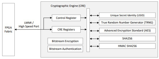
The MachXO5D-NX family incorporates a Root of Trust (RoT) - a secure on-chip area that houses cryptographic keys. It also integrates a hard silicon cryptographic engine supporting advanced encryption standards (AES), hashing algorithms, and a True Random Number Generator (TRNG). Each device possesses a unique secret identity (USID) for enhanced security by safeguarding device identity.

MachXO5-NX DSP cryptographic engine block diagram.
Cryptographic Agility and Robust Protection
These FPGAs boast crypto-agility, allowing them to seamlessly switch between various cryptographic algorithms and methodologies. The chips accommodate Commercial National Security Algorithms (CNSA) for bitstream and user data protection. Supported standards encompass AES-256, ECDSA-384/521, SHA2-256/384/512, and RSA 3072/4096.
The inclusion of dedicated hardware encryption within the silicon eliminates the need to allocate FPGA fabric for security features – a vital aspect for most applications. This design approach not only simplifies development but also maximizes the available FPGA resources for core functionalities.
Power Efficiency and Reliability: The Lattice Nexus Advantage
The MachXO5D-NX family is built upon the Lattice Nexus platform, leveraging a low-power 28-nm fully-depleted silicon-on-insulator (FD-SOI) process. FD-SOI technology significantly reduces leakage current by employing an ultra-thin silicon layer positioned over a buried insulator. This layered architecture minimizes substrate bulk and eliminates the requirement for channel doping, resulting in fully depleted transistors.


